Understanding a circuit board can seem like deciphering a secret map at first, but it's a very learnable skill. For beginners, the key is to break it down into small, manageable concepts.
Here’s a no-nonsense roadmap for reading (and demystifying) a circuit board as a beginner.
1) Safety first
-
If it ever touches mains, don’t power it on while probing unless you know isolation rules.
-
Use a current-limited bench supply when possible (e.g., 5 V @ 0.3 A limit).
2) Gather quick tools
-
Multimeter (continuity + DC volts), fine tweezers, bright light/magnifier.
-
Sticky notes/markers (label rails), phone camera (take sharp photos front/back).
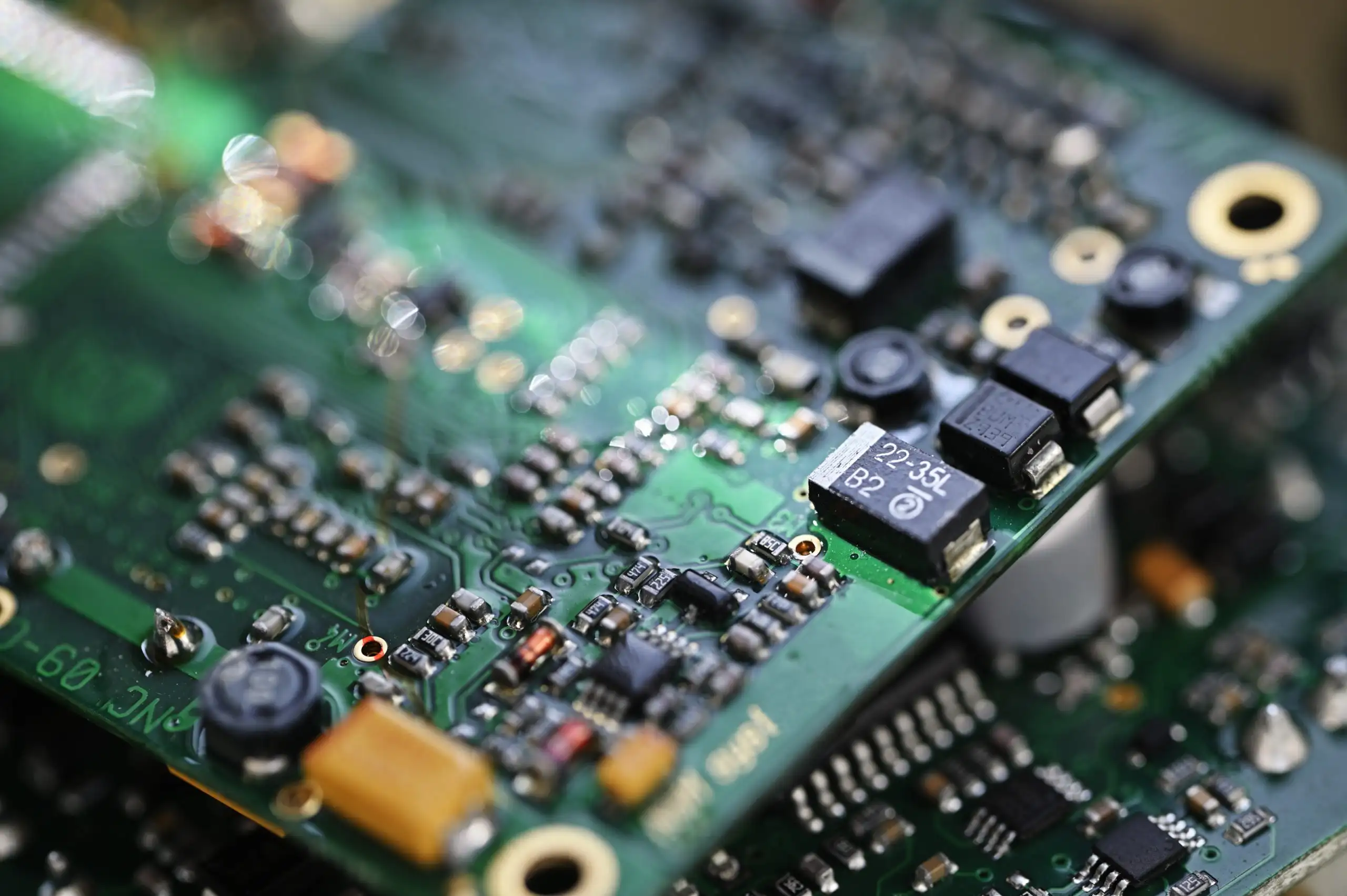
3) Read the silkscreen like a map
Common reference designators:
-
R resistor, C capacitor, L inductor, D diode/LED/TVS, Q transistor,
-
U/IC chips, Y/X crystal/resonator, J/P connector, SW switch, JP jumper,
-
TP test point, FB ferrite bead, F fuse.
Polarity cues: -
Electrolytic cap stripe = negative (usually).
-
Diode bar = cathode.
-
IC dot/notch = pin 1.
-
LED flat side = cathode.
4) Find the power path first
Start at the power connector/USB/barrel jack:
-
Look for F (fuse), D or MOSFET near input (reverse-polarity), and a TVS (surge clamp).
-
Buck/boost regulator = controller IC + big inductor + diode + chunky caps.
-
LDO = tiny regulator near MCU with small caps, no inductor.
-
With power applied, measure rails: common ones are 5 V, 3.3 V, 1.8 V.
Tip: Probe tiny decoupling caps; one side is GND, the other is the rail.
5) Identify “the brain” and its entourage
-
Largest IC is often the MCU/SoC/FPGA. Nearby clues:
-
Crystal/resonator (Y) close to it (8–40 MHz typical for MCU).
-
Flash/EEPROM RAM chips nearby (8-pin SOIC/WSON).
-
Dense clusters of small C around IC pins = decoupling.
-
6) Spot functional zones
Most boards separate into “blocks”:
-
Power (inductors, big caps), Digital (MCU, memory), Analog (op-amps near sensors),
-
RF (shield can/antenna + Pi network), I/O (connectors, level shifters).
Trace from each connector (J) into its block to learn purpose.
7) Recognize high-speed & special signals
-
USB: tight differential pair (D+/D−) from the USB port, tiny ESD array near connector.
-
Ethernet/HDMI: groups of matched-length differential pairs; Ethernet has magnetics (RJ45 with can).
-
Clocks: short, direct traces from crystals to IC.
8) Use continuity mode to “net-hunt”
-
First find GND (USB shield, mounting holes, big copper fills).
-
Beep from a pad to other pads to learn what’s tied together (make your own net labels).
-
Mark TP (test points): often labeled 3V3, 5V, EN, RST, BOOT, SCL, SDA, TX, RX.
9) Decode small passives fast
-
Resistor codes: 3-digit (103 = 10 kΩ), 4-digit (1002 = 10 kΩ), EIA-96 (e.g., 01C → lookup table).
-
Ferrite beads (FB) often sit in series with rails/ports; treat as “RF noise stoppers.”
-
Zero-ohm jumpers (marked “0”) bridge options—great clues for config choices.
10) Build a quick block diagram
-
Draw boxes: Input → Regulator → MCU → Sensors/Drivers → Outputs/Connectors.
-
Add rail labels and key signals (e.g., 3V3, GND, USB D+/D−, I²C, SPI, UART).
This “big picture” makes the part-by-part details click.
11) Power-on sanity checks
-
Bring up with current limit. If it trips, suspect shorts on a rail or wrong polarity parts.
-
Confirm each rail voltage and that the reset line is high (or behaves as expected).
-
LEDs at power-in or near the MCU often show life (power, status, boot).
12) Typical landmarks you’ll start to notice
-
Crystals hugging the MCU, via-stitching walls around RF, serpentine length-matching on high-speed pairs.
-
Analog kept away from digital noise (separate ground islands or moats).
-
ESD arrays right at external connectors.
13) Two mini exercises (great for learning)
-
Arduino-style board: Identify 5 V → 3.3 V regulators, ATmega/ARM MCU, crystal, USB-UART bridge, auto-reset circuit (DTR/CAP to RESET).
-
Phone charger board: Trace AC input → fuse/NTC → bridge rectifier → primary controller → transformer → secondary rectifier → opto-feedback → USB port (observe creepage/isolation!).
14) Common beginner pitfalls
-
Mixing up electrolytic polarity or LED orientation.
-
Probing live mains sections.
-
Assuming two close pads are connected—verify with continuity.
-
Forgetting that ground fills can be on inner layers (multilayer boards can hide nets).
15) What to do if you want to go deeper
-
Photograph both sides, mirror one image, and annotate; you can often reconstruct a partial schematic.
-
Look up IC part markings to get pinouts (then confirm with continuity).
-
If you ever get Gerbers/schematics/BOM, use them to validate your reverse-engineered blocks.